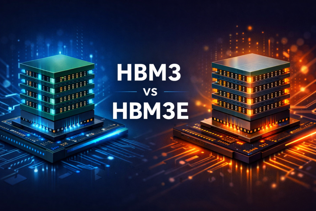
What Is HBM3?
HBM3 represents the third major generation of High Bandwidth Memory, engineered specifically to feed the exploding data appetite of AI accelerators and high-performance computing systems.The official memory standards for HBM are defined by the JEDEC HBM specification, which governs interface speed, signaling requirements, and stack architecture. If HBM2E pushed memory bandwidth into the multi-hundred gigabyte per second range, HBM3 crossed into an entirely new territory enabling nearly a terabyte per second per stack.
But to understand HBM3 properly, you need to see it in architectural context.
HBM3 is still built on the same foundational design principles explained in our deep dive on the Complete HBM Architecture Explained article 3D stacked DRAM dies connected using Through-Silicon Vias (TSVs), placed beside GPUs on a silicon interposer. What changed in HBM3 isn’t the concept it’s the scaling.
Bandwidth Per Stack
HBM3 delivers approximately 819 GB/s per stack, depending on implementation. Multiply that by six stacks and you’re already approaching 5 TB/s of aggregate bandwidth. That’s not a small jump. That’s infrastructure-defining throughput.
Data Rate Per Pin
HBM3 increased per-pin data rate to around 6.4 Gbps, allowing dramatic bandwidth scaling without widening the interface beyond 1024 bits.
Stack Height & Density
Stack heights increased up to 8-high and 12-high configurations, increasing total memory capacity per GPU.
Power Efficiency Improvements
Compared to HBM2E, HBM3 improved energy efficiency per bit transferred a critical factor in hyperscale AI clusters where even small efficiency gains multiply across thousands of accelerators.
AI Workload Positioning
HBM3 became the backbone of modern AI training clusters. Without it, models beyond tens of billions of parameters would face severe bandwidth starvation the exact constraint described in the AI Memory Bottleneck analysis.
HBM3 wasn’t optional. It was necessary.
And then HBM3E arrived.
What Is HBM3E?
HBM3E is not a redesign. It is a refinement but a powerful one.
Think of it like tuning a high-performance engine. The architecture remains the same, but every limit is pushed further.
Evolution from HBM3
HBM3E builds directly on HBM3’s structure but increases operating data rates and improves signal integrity to allow higher sustained throughput.
Increased Data Rate
HBM3E pushes per-pin speeds toward 8–9.2 Gbps, enabling bandwidth per stack to approach or exceed 1 TB/s.
That’s a major leap.
Improved Signal Integrity
Higher data rates require cleaner signaling. HBM3E improves channel equalization, timing margins, and interposer-level routing tolerances.
Higher Stack Density
Manufacturers are increasing stack heights and memory capacity per stack, supporting larger AI models without external spillover.
Efficiency Per Watt
Despite higher speed, energy per bit continues improving a key factor in large-scale AI deployment economics.
Designed for Next-Gen AI Accelerators
HBM3E is purpose-built for next-generation AI GPUs designed to handle trillion-parameter training workloads.
It exists because AI scaling did not slow down.
It accelerated.
Core Architectural Differences Between HBM3 and HBM3E
At a structural level, HBM3 and HBM3E look almost identical. Both rely on 3D-stacked DRAM dies, TSV vertical interconnects, 1024-bit interfaces, and silicon interposers. If you opened the package physically, you wouldn’t immediately see the difference.
But architecture isn’t just about what you see. It’s about limits frequency ceilings, thermal margins, signal integrity tolerances, and energy efficiency curves.
Let’s break this down properly.
Data Rate Per Pin Comparison
HBM3 operates at approximately 6.4 Gbps per pin. That was already a major leap over HBM2E.
HBM3E pushes that toward 8.0–9.2 Gbps per pin, depending on vendor implementation.
That ~30–40% increase may sound incremental. It’s not.
Because bandwidth scales linearly with per-pin speed:
Bandwidth = Bus Width × Data Rate
Since bus width remains 1024 bits per stack, increasing data rate directly increases total throughput.
Bandwidth Per Stack
- HBM3 → ~819 GB/s per stack
- HBM3E → ~1 TB/s+ per stack
Now multiply that by 8 stacks in high-end GPUs:
- HBM3 → ~6.5 TB/s
- HBM3E → ~8 TB/s+
That’s infrastructure-level bandwidth.
Maximum Stack Height
HBM3 supports up to 8-high and 12-high stacks.
HBM3E pushes capacity further with higher-density dies and improved stacking techniques.
This directly impacts how large a model can reside in local GPU memory before spilling into slower tiers.
Thermal Tolerance
Higher speeds generate more heat. HBM3E incorporates:
- Improved voltage scaling
- Better thermal handling
- Refined signaling margins
Without this, pushing 9+ Gbps per pin would destabilize performance.
Energy Efficiency Per Bit
Despite higher speed, energy per bit does not scale proportionally. Engineering improvements in signal integrity allow HBM3E to maintain competitive efficiency.
HBM3 vs HBM3E Comparison Table
| Feature | HBM3 | HBM3E |
|---|---|---|
| Data Rate Per Pin | ~6.4 Gbps | ~8–9.2 Gbps |
| Bandwidth Per Stack | ~819 GB/s | ~1 TB/s+ |
| Max Stack Height | 8–12 dies | 12+ high-density dies |
| Thermal Optimization | Advanced | Further improved |
| Efficiency Per Bit | Improved vs HBM2E | Optimized for higher speeds |
| AI Positioning | Current Gen AI | Next-Gen AI Scaling |
The architecture didn’t change.
The ceiling did.
Bandwidth Scaling in AI GPUs
Now let’s connect memory specs to real GPU scaling.
Because raw bandwidth numbers mean nothing unless we translate them into AI throughput.
6-Stack vs 8-Stack Configuration
Most AI GPUs integrate either:
- 6 HBM stacks
- 8 HBM stacks
Let’s do simple math.
If using HBM3:
6 stacks × 819 GB/s ≈ 4.9 TB/s
8 stacks × 819 GB/s ≈ 6.5 TB/s
If using HBM3E:
6 stacks × 1 TB/s ≈ 6 TB/s
8 stacks × 1 TB/s ≈ 8 TB/s
That’s a difference of more than 1.5 TB/s in top configurations.
Total Bandwidth Math and FLOPS Utilization
Why does this matter?
Because AI accelerators often hit a limit where compute cores sit idle waiting for data. This is the exact constraint discussed in our analysis of the AI Memory Bottleneck.
Higher bandwidth means:
- Higher tensor streaming rate
- Better compute saturation
- Reduced stall cycles
- Improved FLOPS utilization
In large-scale training jobs, even a 10–15% increase in effective utilization can reduce training time by days.
AI Training Throughput Impact
Training throughput depends on how fast gradients, activations, and parameters move in and out of memory.
If bandwidth increases:
- Batch sizes increase
- Parallel tensor operations scale
- Data pipeline congestion reduces
HBM3E doesn’t just add speed.
It reduces idle compute.
And idle compute is wasted capital.
AI Performance Impact
Now we translate architecture into model-level consequences.
LLM Training Throughput
Large Language Models with hundreds of billions of parameters require enormous sustained memory bandwidth.
HBM3 already enabled 70B–175B parameter training at scale.
HBM3E extends that headroom.
Higher bandwidth means:
- Larger model shards per GPU
- Reduced memory pressure
- Better scaling efficiency in distributed setups
This improves end-to-end training throughput.
Inference Acceleration
Inference workloads may not saturate bandwidth like training does, but they benefit from:
- Faster weight loading
- Reduced latency under high concurrency
- Improved throughput in serving clusters
HBM3E particularly benefits high-throughput inference systems.
Multi-GPU Scaling Impact
When scaling across nodes, memory bandwidth per GPU determines how efficiently each unit processes its partition.
Higher local bandwidth reduces cross-node communication pressure.
This improves cluster-level scaling efficiency.
Large Parameter Model Support
With increased stack density and bandwidth, HBM3E allows:
- Larger parameter models per accelerator
- Fewer off-chip memory spills
- Better performance per node
This becomes critical for trillion-parameter ambitions.
Power & Thermal Differences
Now let’s address the elephant in the room.
Higher speed usually means higher power.
But it’s more nuanced.
Voltage Optimization
HBM3E refines voltage control to maintain efficiency even at higher speeds. Improved signaling reduces unnecessary energy loss.
Heat Density
Higher throughput increases heat concentration near GPU cores.
Data centers must compensate with:
- Advanced cooling systems
- Liquid cooling loops
- Optimized airflow
This ties directly into infrastructure economics, as discussed in the AI Infrastructure Memory Energy Costs analysis.
Data Center Implications
In hyperscale environments:
- 5% power difference per GPU scales massively
- Cooling cost becomes a dominant factor
HBM3E improves performance per watt, but total system design must evolve alongside it.
Cost & Supply Considerations
Performance is one side of the equation. Cost and supply determine what actually ships at scale.
And this is where the HBM3 vs HBM3E conversation becomes strategic.
Manufacturing Complexity
Both HBM3 and HBM3E rely on:
- TSV drilling
- Die thinning
- 3D stacking
- Silicon interposers
- Advanced packaging
But HBM3E pushes tighter electrical tolerances and higher frequency signaling. That means:
- Stricter quality control
- Lower acceptable defect margins
- More complex validation cycles
Even small signal instability at 9+ Gbps per pin can create reliability issues. So fabrication precision becomes even more critical.
The broader structural challenges in HBM manufacturing are explained in the HBM Semiconductor Industry analysis, but HBM3E intensifies those pressures.
Yield Challenges
Higher stack heights + higher data rates = higher defect sensitivity.
If one die fails in a 12-high stack, the entire stack is compromised. Now add tighter signal timing windows yield becomes even more sensitive.
Lower yield means:
- Higher cost per stack
- Limited early supply
- Premium pricing
That’s why HBM3E initially appears in top-tier accelerators only.
Industry Adoption
HBM3 is already widely deployed in production AI GPUs.
HBM3E adoption is ramping in next-generation accelerators designed specifically for ultra-large AI workloads.
Memory vendors aggressively pushing HBM3E include:
- SK Hynix
- Samsung
- Micron
But supply constraints remain a real bottleneck. In fact, memory allocation has become one of the key gating factors in AI hardware scaling.
Which Vendors Use HBM3E?
Next-generation AI accelerators targeting trillion-parameter scale increasingly integrate HBM3E to avoid bandwidth ceilings.
However, many currently deployed clusters still rely on HBM3 due to availability and cost considerations.
HBM3E is not just a spec bump.
It’s a supply chain strategy.
Which One Should AI Infrastructure Use?
This is where theory meets deployment reality.
The answer depends on timing and objective.
If Deploying Today → HBM3
If you’re building infrastructure right now and:
- Running 70B–175B parameter models
- Operating within established cluster architectures
- Managing capital expenditure carefully
HBM3 is fully capable.
It already provides multi-terabyte per second bandwidth. For many AI workloads, compute limits may be reached before memory becomes the next bottleneck.
HBM3 offers:
- Mature ecosystem
- Proven stability
- Better availability
- Lower cost relative to HBM3E
If Scaling Next-Gen Clusters → HBM3E
If you are:
- Planning trillion-parameter training
- Building next-gen AI research clusters
- Targeting maximum FLOPS utilization
HBM3E provides valuable headroom.
Higher bandwidth per stack reduces:
- Compute stall
- Cross-node communication pressure
- Memory congestion
It future-proofs infrastructure investments.
ROI Discussion
Here’s the real question:
Does a 15–25% bandwidth increase justify higher cost?
In hyperscale AI environments, even:
- 5% training time reduction
- 10% improved GPU utilization
Can translate into millions in savings over time.
So ROI depends on workload intensity and cluster scale.
HBM3E isn’t mandatory for everyone.
But for bleeding-edge AI scaling, it becomes strategically attractive.
Future Roadmap: Beyond HBM3E
HBM3E is not the end of the roadmap.
It’s a stepping stone.
Toward 1.2–1.5 TB/s Per Stack
Industry roadmaps indicate future iterations targeting 1.2 to 1.5 TB/s per stack.
At that point:
8 stacks × 1.5 TB/s = 12 TB/s total bandwidth.
That’s almost unimaginable compared to early HBM generations.
Stack Height Growth
Expect:
- Higher layer counts
- Increased density DRAM dies
- Improved hybrid bonding techniques
More layers mean more capacity but also greater thermal complexity.
Hybrid Bonding
Hybrid bonding reduces micro-bump size and improves interconnect density. This enables:
- Better signal integrity
- Lower resistance
- Higher frequency scaling
It’s likely to play a major role in post-HBM3E generations.
AI Scaling Pressure
AI models are not stabilizing in size.
They are expanding.
From billions → hundreds of billions → trillions.
Memory bandwidth scaling must match compute scaling, or the memory wall returns a phenomenon deeply analyzed in the AI Memory Bottleneck discussion.
The roadmap is clear:
Bandwidth must grow faster than compute stalls.
And HBM evolution is the mechanism enabling that.
FAQs
1. Is HBM3E backward compatible with HBM3?
HBM3E is architecturally similar to HBM3, but compatibility depends on GPU controller design. Accelerators must be designed to support higher data rates and signaling requirements.
2. How much faster is HBM3E in AI training?
HBM3E can provide roughly 15–25% higher bandwidth per stack compared to HBM3, which can translate into improved training throughput depending on workload intensity.
3. Does HBM3E increase GPU power consumption?
While peak power may increase due to higher data rates, efficiency per bit remains competitive. Overall system design determines total power impact.
4. Which GPUs use HBM3E?
Next-generation AI accelerators targeting large-scale training increasingly integrate HBM3E to maximize bandwidth headroom.
5. Is HBM3E necessary for LLM training?
Not always. Many current LLM workloads run effectively on HBM3. However, extremely large models and next-gen scaling efforts benefit significantly from HBM3E’s increased bandwidth.
Conclusion
HBM3 and HBM3E share the same architectural DNA 3D stacking, TSV connectivity, 1024-bit interfaces, and silicon interposers. The difference lies not in structure, but in limits.
HBM3 delivers nearly 819 GB/s per stack and powers current-generation AI accelerators effectively.
HBM3E pushes that toward or beyond 1 TB/s per stack, increasing per-pin data rates, improving signal integrity, and extending the bandwidth ceiling for next-generation AI systems.
For today’s large-scale deployments, HBM3 remains highly capable and cost-efficient.
For tomorrow’s trillion-parameter ambitions, HBM3E offers critical performance headroom.
The decision is not purely technical.
It is strategic.
As AI models scale and infrastructure investments grow, memory bandwidth becomes the defining constraint.
And in that race, HBM3E is simply the next step forward.