
What Is High Bandwidth Memory (HBM)?
High Bandwidth Memory (HBM) is a 3D-stacked DRAM architecture designed to deliver extremely high data throughput with lower power consumption compared to traditional memory technologies.
The official HBM interface specifications are defined by the JEDEC HBM standard, which governs stack architecture, signaling speeds, and memory channel design.
Let’s break that down in practical terms.
Modern AI systems don’t struggle because they lack compute power. They struggle because they can’t move data fast enough. That bottleneck is exactly where HBM steps in. Unlike conventional DDR memory, which spreads chips across a motherboard with long electrical traces, HBM stacks memory vertically and places it right next to the processor using advanced packaging.
If you want a deeper foundational explanation, you can explore this detailed guide on what is HBM, where the conceptual framework is explained step by step.
Instead of increasing clock speed aggressively (which increases heat and power), HBM increases bus width dramatically. We’re talking about a 1024-bit interface per stack. That’s not a minor tweak that’s a structural shift.
Traditional DRAM becomes insufficient for AI because AI workloads, especially large language models and transformer architectures, demand continuous, high-volume tensor movement. GPUs process massive matrices, and every millisecond of memory delay reduces effective compute utilization. This imbalance is commonly referred to as the memory wall problem, which is explored in depth in this analysis of the AI memory bottleneck.
AI workloads are fundamentally data-movement intensive. Training a model isn’t just about computing weights it’s about reading and writing terabytes of parameters repeatedly. When memory bandwidth falls short, FLOPS sit idle. And idle compute is wasted investment.
HBM isn’t just “better RAM.” It’s an architectural redesign aimed specifically at solving bandwidth starvation in AI infrastructure memory systems. If you’re comparing technologies, this breakdown of HBM vs DRAM and HBM vs GDDR for AI workloads highlights why HBM dominates modern accelerators.
HBM exists because AI forced memory architecture to evolve.
The Memory Wall Problem in AI Systems
The memory wall problem occurs when compute performance grows exponentially but memory bandwidth fails to keep pace.
Imagine owning a sports car capable of 300 km/h but driving it on a one-lane road clogged with traffic. That’s exactly what happens in AI accelerators today.
CPUs traditionally operate with relatively balanced compute-to-memory ratios. GPUs, however, are massively parallel machines. A modern AI GPU can deliver tens of teraflops even petaflops of compute performance. But without proportional bandwidth, those cores stall.
Large Language Models (LLMs) amplify this issue. A 70B parameter model requires hundreds of gigabytes per second during inference and multiple terabytes per second during training. The memory demand scales linearly with parameters, but compute scales even faster.
This creates a FLOPS-to-bandwidth imbalance the exact issue explained in this technical breakdown of the AI memory bottleneck.
Let’s introduce a core formula:
Bandwidth = Bus Width × Data Rate × Channels
If your bus width is narrow (like DDR’s 64-bit interface), even increasing frequency won’t deliver enough bandwidth without skyrocketing power usage. HBM solves this not by racing the clock but by widening the highway.
For example:
- DDR5: 64-bit interface
- GDDR6: 32-bit per chip
- HBM: 1024-bit per stack
That’s not incremental improvement that’s structural transformation.
AI systems don’t primarily need ultra-low latency random access. They need sustained throughput for tensor streaming. That’s why HBM prioritizes wide I/O architecture over frequency scaling.
If you also care about energy economics at scale, this article on AI infrastructure memory energy costs explains why bandwidth inefficiency directly impacts data center spending.
The memory wall isn’t theoretical.
It’s the defining architectural challenge of modern AI hardware.
Core HBM Architecture Overview
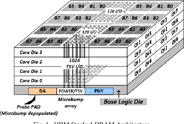
HBM is physically structured as vertically stacked DRAM dies connected through microscopic vertical interconnects and placed on a silicon interposer alongside the GPU.
Now let’s visualize it.
Instead of placing memory chips around a board, HBM stacks 4, 8, or even 12 DRAM layers vertically. At the bottom sits a base logic die. Above it are multiple DRAM memory dies. These layers are connected using Through-Silicon Vias (TSVs), forming a single compact cube-like memory stack.
Each layer communicates vertically rather than across long motherboard traces.
Here’s how the structure flows:
- DRAM Layers – Store actual data bits.
- Base Logic Die – Manages memory control and signal routing.
- Micro-Bumps – Provide ultra-dense electrical connections between layers.
- Silicon Interposer – Connects memory stacks to the GPU die.
Think of it like a skyscraper instead of suburban houses. Instead of spreading memory out horizontally, HBM builds upward.
The 3D stacking reduces signal distance dramatically. Shorter distance means:
- Lower latency
- Lower energy per bit transfer
- Higher signal integrity
- Massive parallel data flow
A diagram would show the GPU die placed beside multiple HBM stacks on a shared silicon interposer. TSVs run vertically through each memory die, while thousands of micro-bumps connect the stack to the interposer below.
If you want a more semiconductor-focused perspective, this overview of the HBM semiconductor industry explains how fabrication complexity shapes the market.
Without stacking, achieving terabytes per second bandwidth would require impractical power consumption.
HBM’s architecture is not just compact it is engineered for parallelism at a physical level.
Through-Silicon Via (TSV) Technology
Through-Silicon Vias (TSVs) are vertical electrical connections that pass directly through silicon dies to enable 3D stacking.
Instead of routing signals around a chip, TSVs drill microscopic copper-filled holes straight through it. This allows signals to travel vertically between layers with minimal resistance.
Why does this matter?
Signal path shortening.
In traditional memory, signals travel horizontally across PCB traces. That distance increases capacitance and power draw. TSVs reduce that path to micrometers instead of centimeters.
Shorter path equals:
- Lower latency
- Reduced energy consumption
- Higher bandwidth density
- Improved signal synchronization
TSVs are not optional add-ons. They are foundational to complete HBM architecture. In fact, this deep technical exploration of TSV in HBM AI performance explains how vertical connectivity directly increases throughput per watt.
From a performance perspective, TSVs allow thousands of vertical connections per stack. That density enables the 1024-bit interface per HBM stack.
From an energy perspective, reduced trace length lowers power per bit transfer significantly. In AI data centers, where energy cost scales massively, this becomes critical. For a sustainability angle, read about the AI hardware carbon footprint and how memory efficiency plays a central role.
However, TSV manufacturing is complex. Drilling, insulating, and filling vias with copper must be precise. Even minor defects reduce yield. That’s one reason HBM remains expensive.
But without TSVs, true 3D memory stacking would be impossible.
TSVs transform memory from flat circuitry into vertical infrastructure.
Silicon Interposer Explained
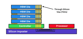
A silicon interposer is a thin silicon layer that electrically connects the GPU and multiple HBM stacks in a 2.5D package configuration.
HBM cannot sit directly on a motherboard like DDR. It needs extremely dense routing — far beyond what organic substrates can support.
Enter the interposer.
Think of it as a high-speed silicon bridge. It sits beneath both the GPU die and the HBM stacks. Thousands of ultra-fine metal traces run across it, enabling massive data exchange at high bandwidth.
This is called 2.5D packaging not fully 3D integrated, but more advanced than traditional packaging.
If you want a detailed packaging explanation, this guide on the silicon interposer in HBM walks through routing density and structural design.
Why is proximity important?
Because bandwidth scales with parallel connections. The closer memory sits to compute, the more wires you can pack between them.
Interposers enable:
- Ultra-wide data buses
- Signal integrity at high speeds
- Reduced electromagnetic interference
- Massive routing density
Without interposers, you simply could not support terabytes per second bandwidth between GPU and memory.
This architecture minimizes signal distance, optimizes bandwidth flow, and improves parallel data transfer at a structural level.
It’s not a packaging trick.
It’s a performance enabler.
Memory Channels & Bus Width in HBM
HBM achieves massive bandwidth by using an ultra-wide 1024-bit interface per stack combined with multiple parallel memory channels.
Now pause for a second and imagine traffic flow.
Would you rather drive on a narrow two-lane road at 200 km/h, or a 20-lane highway at 100 km/h? Even if each car moves slightly slower, the total number of cars reaching the destination per second is dramatically higher on the wider highway. That’s exactly how HBM thinks about performance.
Instead of chasing extreme clock speeds like DDR and GDDR memory, HBM widens the data path.
Each HBM stack typically includes:
- 8 or 16 independent memory channels
- 128-bit interface per channel
- Total 1024-bit interface per stack
Compare that to:
- DDR5 → 64-bit interface
- GDDR6 → 32-bit per chip
That’s not just wider. It’s architecturally different.
Parallelism is the real superpower here. Each memory channel operates independently, allowing simultaneous data transfers. That means AI accelerators can stream tensors continuously without waiting for serialized memory access.
This is one of the reasons HBM outperforms alternatives in AI workloads, as discussed in this comparison of HBM vs GDDR for AI workloads. GDDR can achieve high speeds, but it relies heavily on frequency scaling. HBM achieves similar or greater throughput through structural width.
The scaling mechanism works like this:
Total Bandwidth = Bandwidth per Stack × Number of Stacks
So if one HBM3 stack delivers ~819 GB/s, six stacks can push close to 5 TB/s.
That level of sustained throughput is what keeps thousands of GPU cores busy during AI training.
HBM doesn’t just move data faster.
It moves more data at once.
That’s the distinction that matters.
Latency vs Bandwidth Tradeoff
HBM prioritizes bandwidth over ultra-low latency because AI workloads require sustained throughput more than rapid random-access response time.
Here’s where confusion often creeps in.
People hear “high-performance memory” and assume ultra-low latency. But performance isn’t just about how fast the first byte arrives. It’s about how much data can flow continuously.
Think of it like water pipes.
Latency is how long it takes for water to start flowing after you turn the tap.
Bandwidth is how much water flows per second once it’s running.
AI training doesn’t sip water.
It floods the system with tensor operations.
Why Throughput Matters More in AI
Transformer models repeatedly stream:
- Model parameters
- Activations
- Gradients
- Intermediate tensor outputs
These aren’t tiny, random reads. They’re massive, structured matrix operations.
If bandwidth drops:
- GPU cores stall
- FLOPS utilization decreases
- Training time increases
- Infrastructure cost rises
This inefficiency ties directly into the broader AI memory bottleneck problem.
Let’s revisit the bandwidth formula:
Bandwidth = Bus Width × Data Rate × Channels
Example:
- DDR5: 64-bit × 6.4 Gbps ≈ 51.2 GB/s
- HBM3: 1024-bit × ~6.4 Gbps ≈ 819 GB/s per stack
Multiply that by 6 stacks:
819 GB/s × 6 ≈ 4.9 TB/s
Latency differences may only be in tens of nanoseconds, but throughput difference is exponential.
Cache Interaction in GPUs
Modern GPUs include large L2 and shared memory caches. HBM feeds those caches at high rates. Once data enters on-chip SRAM, ultra-low latency becomes less critical.
HBM acts as a high-capacity streaming buffer.
It’s optimized for throughput, not microsecond bragging rights.
And in AI economics, throughput wins every time.
Power Consumption & Thermal Challenges
HBM reduces power per bit transferred, but its dense 3D structure introduces significant thermal management complexity.
There’s a tradeoff here and it’s important to understand both sides.
Power Per Bit Transfer
Because HBM sits extremely close to the GPU on the silicon interposer, signal traces are dramatically shorter than in traditional board-level memory.
Shorter traces mean:
- Lower capacitance
- Reduced voltage swing
- Less signal degradation
- Lower energy per transferred bit
Compared to DDR routed across a motherboard, HBM is significantly more energy efficient per unit of data.
At AI data center scale, that efficiency matters enormously. Thousands of accelerators running 24/7 multiply even small power improvements into massive operational savings.
This is explored further in the breakdown of AI infrastructure memory energy costs and its connection to system-wide efficiency.
There’s also a sustainability angle. Memory efficiency directly affects the AI hardware carbon footprint, especially in hyperscale deployments.
Thermal Stacking Challenges
Now the harder part.
HBM stacks multiple DRAM dies vertically. That means:
- Heat from upper layers must travel downward
- Thermal dissipation becomes uneven
- Cooling becomes more complex
Unlike DDR modules spaced apart, HBM stacks sit right next to a high-power GPU core. This creates a dense thermal hotspot.
Advanced cooling becomes mandatory:
- Vapor chambers
- Direct-to-chip liquid cooling
- Optimized airflow design
As discussed in sustainable AI hardware strategies, packaging innovation and thermal optimization are becoming just as important as compute scaling.
HBM improves efficiency per bit.
But it demands smarter cooling infrastructure.
Efficiency and engineering complexity grow together.
GPU Integration: How HBM Connects to AI Accelerators
HBM integrates directly on-package with GPUs, enabling ultra-wide parallel memory interfaces that traditional board-level memory cannot achieve.
This is where architectural theory becomes real system advantage.
On-Package Memory Architecture
HBM stacks are mounted on the same silicon interposer as the GPU die. This proximity enables thousands of parallel signal connections something impossible through motherboard routing.
Instead of signals traveling through:
- DIMM slots
- Long copper traces
- Multiple board layers
Everything happens within millimeters.
This dramatically reduces electrical noise and increases bandwidth density.
Multi-Stack Configuration
AI accelerators typically include 4, 6, or 8 HBM stacks.
Each stack contributes:
- 1024-bit interface
- Independent memory channels
- Dedicated bandwidth
Combined, this forms a massive shared memory pool.
Modern accelerators often reach:
- 80–120 GB total HBM capacity
- 3–5 TB/s total bandwidth
This pool feeds tensor cores continuously during training. Without it, compute units would starve the exact issue described in the AI memory bottleneck discussion.
NVLink and Multi-GPU Scaling
While HBM provides ultra-fast local memory bandwidth, large AI clusters require GPUs to communicate across nodes. High-speed interconnect technologies such as NVIDIA NVLink extend bandwidth beyond a single accelerator.
HBM serves as high-speed local memory.
NVLink enables accelerator-to-accelerator data exchange at extremely high throughput.
Together, they create a hierarchical bandwidth system:
Local bandwidth (HBM) + Distributed bandwidth (NVLink).
Without HBM, GPUs would starve locally.
Without high-speed interconnects, multi-GPU scaling would collapse.
Modern AI infrastructure depends on both.
Evolution of HBM Generations
HBM has evolved across multiple generations, each dramatically increasing bandwidth, efficiency, and stack density.
Let’s look at the progression.
HBM1
- ~128 GB/s per stack
- 4-layer stacks
- First commercial deployment
HBM2
- ~256 GB/s per stack
- Higher stack density
- Improved signaling
HBM2E
- ~400+ GB/s per stack
- Better energy efficiency
- Increased data rates
HBM3
- ~819 GB/s per stack
- More channels
- Significant power optimization
HBM3E
- Approaching or exceeding 1 TB/s per stack
- Higher thermal tolerance
- Greater efficiency per watt
Across generations, improvements include:
- Increased stack height (up to 12+ layers)
- Higher bandwidth per pin
- Improved manufacturing precision
- Better signal integrity
This rapid evolution mirrors AI scaling demands. As models grew from millions to billions — and now trillions memory bandwidth had to scale alongside compute.
For broader industry context, the article on the HBM semiconductor industry explains how supply chain and fabrication complexity shape generational advancement.
HBM’s roadmap is directly tied to AI’s exponential growth curve.
Limitations of HBM
HBM delivers extraordinary bandwidth, but it is not a perfect solution. Every architectural leap introduces new engineering tradeoffs. If we only talk about performance without addressing constraints, we miss the full picture.
Let’s unpack the real-world limitations.
Manufacturing Complexity
HBM production is significantly more complex than conventional DRAM manufacturing. It involves:
- Precision die thinning
- Through-Silicon Via (TSV) drilling and copper filling
- Multi-die vertical stacking
- Micro-bump bonding
- Silicon interposer fabrication
Each step must align at microscopic precision. A tiny defect in alignment can compromise signal integrity or thermal performance. Unlike traditional DRAM chips placed independently on a PCB, HBM components are tightly integrated into a single 2.5D package.
This complexity is one reason the HBM semiconductor industry operates with higher barriers to entry compared to commodity memory manufacturing.
Yield Challenges
When stacking multiple dies vertically, the probability of defects increases. If one die in the stack fails, the entire stack can become unusable.
Think about it like stacking fragile glass plates. If even one plate cracks, the entire tower becomes unstable.
Lower yield directly increases production cost. This is one of the main reasons HBM remains concentrated in high-end AI accelerators rather than mainstream consumer systems.
Cost Factors
HBM is significantly more expensive than DDR or GDDR due to:
- Advanced packaging
- Silicon interposers
- Low production yield
- Specialized fabrication equipment
The cost structure makes it viable primarily for data centers and AI infrastructure, where bandwidth efficiency justifies the premium.
Capacity Constraints
HBM is optimized for bandwidth, not massive capacity. While modern GPUs may offer 80–120 GB of HBM, enterprise servers can host terabytes of DDR memory.
That’s why HBM functions as high-speed working memory, not large-scale storage. AI systems often combine HBM with other memory tiers to balance capacity and throughput.
HBM is powerful — but specialized.
It solves the bandwidth problem, not every memory problem.
Future of High Bandwidth Memory in AI
The future of HBM is directly tied to the future of artificial intelligence. As AI models scale, memory bandwidth must scale alongside them. Compute alone is no longer the limiting factor.
Bandwidth is.
Advanced 3D Packaging
Future generations of HBM will likely increase:
- Stack height (more DRAM layers)
- Bandwidth per pin
- Thermal dissipation efficiency
- Interposer routing density
Engineers are exploring improved 3D packaging techniques to reduce thermal hotspots while maintaining vertical connectivity.
This packaging evolution aligns closely with trends in sustainable AI hardware, where performance improvements must coexist with energy efficiency goals.
Chiplets and Modular AI
AI accelerators are moving toward chiplet-based designs rather than monolithic dies. Smaller compute tiles can be interconnected using high-speed links while sharing HBM stacks.
This modular approach enables:
- Better yield
- Flexible scaling
- Customizable performance tiers
HBM integrates naturally into chiplet ecosystems because it already operates in a tightly coupled on-package configuration.
Co-Packaged Optics
As AI clusters scale across racks and data centers, electrical interconnects face limitations. Co-packaged optics integrating optical communication closer to compute and memory may reduce data transfer bottlenecks beyond the package level.
While HBM handles local bandwidth, optical solutions could extend that efficiency across nodes.
AI Scaling Demands
Model sizes continue growing from billions to trillions of parameters. Each scale jump multiplies memory bandwidth requirements.
If compute doubles but bandwidth does not, the memory wall returns.
Future HBM generations must:
- Exceed multi-terabyte per second throughput
- Improve energy efficiency per bit
- Reduce manufacturing complexity
- Increase stack capacity
The pressure is relentless.
HBM is no longer optional in AI infrastructure. It is foundational to modern accelerator design.
The companies that solve bandwidth scaling most efficiently will define the next era of AI hardware leadership.
FAQs
1. Why is HBM better than DDR for AI workloads?
HBM provides significantly higher bandwidth through 3D stacking and ultra-wide interfaces. AI workloads require sustained tensor streaming, which DDR’s narrow bus architecture struggles to support efficiently.
2. Does HBM reduce latency compared to traditional DRAM?
HBM slightly reduces signal delay due to shorter trace distances, but its primary advantage is bandwidth, not ultra-low latency. It is optimized for throughput rather than random-access speed.
3. How much bandwidth does HBM3 provide?
HBM3 delivers approximately 819 GB/s per stack. With multiple stacks integrated into modern GPUs, total bandwidth can exceed 3–5 TB/s.
4. Why is HBM expensive?
HBM requires complex TSV manufacturing, vertical stacking, die thinning, and silicon interposers. These processes reduce yield and increase production costs compared to conventional memory technologies.
5. Can HBM replace traditional system RAM?
No. HBM is optimized for high bandwidth, not massive capacity. It serves as ultra-fast working memory for GPUs and AI accelerators, while DDR remains better suited for large-scale system memory capacity
Conclusion
High Bandwidth Memory is not simply an upgrade over traditional DRAM. It represents a structural redesign of memory architecture created specifically to overcome the memory wall in AI systems.
Through 3D stacking, Through-Silicon Vias, silicon interposers, and ultra-wide 1024-bit interfaces, HBM enables terabytes-per-second data transfer directly beside AI accelerators. It reduces signal distance, improves energy efficiency, maximizes parallelism, and sustains the data flow required for modern tensor-heavy workloads.
Without HBM, today’s large language models, generative AI systems, and high-performance training clusters would operate far below their theoretical compute capacity. GPUs would stall. FLOPS would idle. Infrastructure costs would skyrocket.
Yes, HBM introduces manufacturing complexity and higher cost. Yes, thermal management becomes more demanding. But those challenges exist because the architecture is pushing physical limits.
In modern AI infrastructure, compute power alone no longer defines performance.
Memory bandwidth does.
And HBM is the architectural answer to that reality.