Introduction: The Microscopic Structure Enabling Modern AI
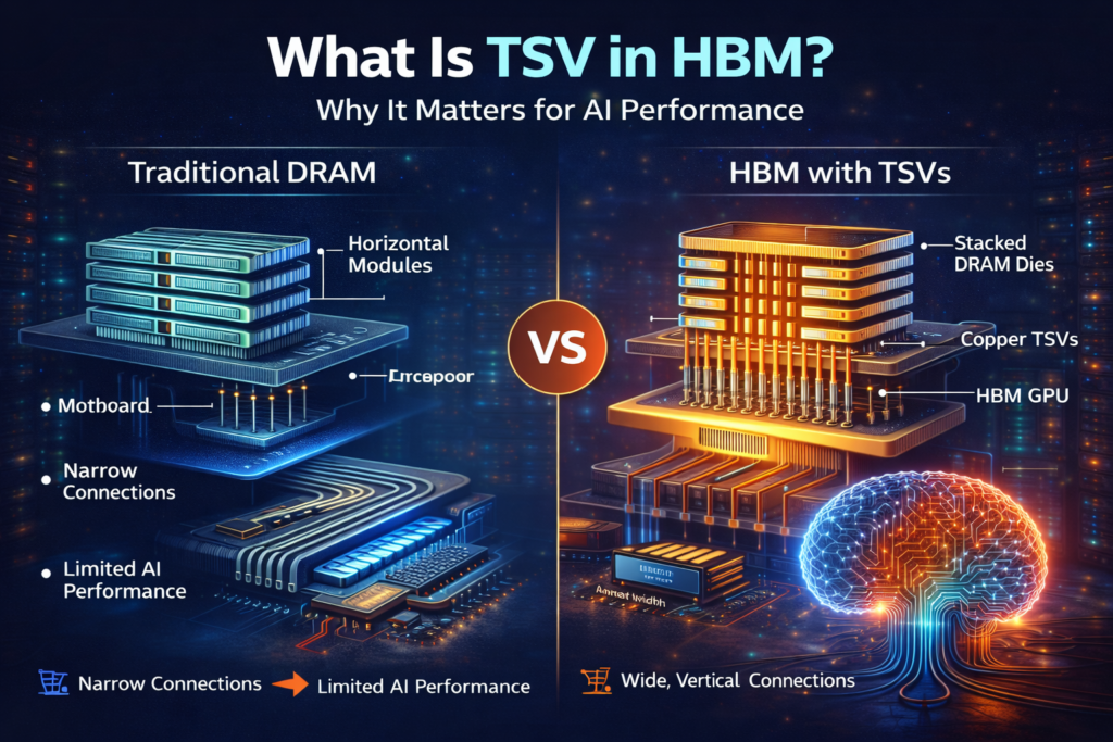
Through-Silicon Via (TSV) is a vertical copper-filled electrical connection that passes through a silicon die, enabling stacked semiconductor layers to communicate with extremely high bandwidth and reduced signal distance.
Modern AI systems are not limited by compute power alone. They are limited by how efficiently data moves between memory and processors. As AI models scale into billions and trillions of parameters, memory bandwidth becomes the primary performance constraint.
High Bandwidth Memory (HBM) solves this constraint through vertical stacking, a shift that is explained in detail in our guide on High Bandwidth Memory in AI. TSV is the structural mechanism that makes that stacking possible.
Without TSV, HBM cannot function. Without HBM, large-scale AI training systems built by companies like NVIDIA and AMD would suffer severe memory bottlenecks.
TSV is not a supporting component. It is an architectural enabler.
The Architectural Problem TSV Solves
Traditional DRAM is built using planar architecture. Memory modules sit horizontally on a motherboard and connect to processors through narrow electrical interfaces.
This design introduces several limitations:
- Limited bus width
- Long signal travel distance
- Increased energy per bit transferred
- Pin-count constraints on processors
As AI workloads evolved toward parallel tensor computation, horizontal memory scaling became inefficient.
Increasing clock speed raises power consumption and heat. Increasing physical bus width requires more board space and pins.
TSV changes the scaling strategy.
Instead of increasing frequency, it increases vertical connection density.
This shift from frequency scaling to interconnect density scaling is one of the most important architectural transitions in AI-era hardware.
What Exactly Is a Through-Silicon Via?
A Through-Silicon Via is a microscopic vertical channel etched through a silicon wafer, insulated, and filled with conductive material (usually copper), allowing signals to pass vertically between stacked dies.
Typical TSV dimensions:
- Diameter: 5 to 10 micrometers
- Depth: 30 to 100 micrometers
- Count per HBM stack: often thousands
In a single HBM stack, TSV arrays create extremely dense vertical interconnections between memory layers.
Functionally, TSV enables:
- Vertical signal transmission
- Reduced parasitic resistance
- Lower latency variance
- Higher interconnect density
This transforms memory from a flat 2D layout into a true 3D structure.
How TSV Enables High Bandwidth Memory (HBM)
HBM consists of multiple DRAM dies stacked vertically and placed adjacent to a processor on a silicon interposer, as discussed in our detailed explanation of what High Bandwidth Memory is and why AI needs it.
TSVs provide the vertical communication paths between those stacked layers.
In modern HBM3 designs:
- Memory stacks may contain 8 to 12 DRAM layers
- Each stack can deliver over 800 GB/s of bandwidth
- Multiple stacks can exceed several terabytes per second
This bandwidth is not achieved through extreme clock speeds. It is achieved through interface width.
HBM uses extremely wide buses, often 1024 bits or more per stack.
TSV enables that width without expanding footprint.
This is why GPUs from NVIDIA (such as data center accelerators) and advanced AI systems rely heavily on TSV-based HBM.
TSV and AI Workload Behavior
AI workloads are dominated by parallel tensor operations. During training:
- Thousands of compute cores request data simultaneously
- Parameter updates occur continuously
- Memory access must be consistent under load
If memory cannot sustain throughput, compute units stall. This phenomenon is known as compute starvation.
TSV-based HBM reduces compute starvation by:
- Shortening signal paths
- Increasing parallel data channels
- Reducing energy per bit transferred
The result is higher GPU utilization.
In AI systems, effective performance depends more on sustained memory throughput than peak theoretical FLOPS.
TSV directly supports sustained throughput.
TSV vs Traditional Memory Interconnects
Traditional DRAM uses:
- Horizontal PCB traces
- Edge connectors
- Narrower interfaces
Scaling bandwidth requires increasing frequency, which increases heat and power consumption.
TSV-based memory uses:
- Vertical copper interconnects
- Dense micro-bump connections
- Wide parallel interfaces
Instead of scaling frequency, it scales interconnect density.
This makes TSV-based designs more efficient for AI-scale workloads.
TSV vs Wire Bonding and Alternative Approaches
Before TSV became mainstream, wire bonding was commonly used to connect stacked dies.
Wire bonding limitations:
- Longer signal paths
- Limited density
- Lower bandwidth scalability
TSV advantages:
- Direct vertical signal path
- Higher interconnect density
- Lower electrical resistance
- Better scalability for 3D stacking
Compared to chiplet-based horizontal interconnect approaches, TSV offers tighter integration between memory layers.
However, TSV introduces higher fabrication complexity.
Manufacturing Complexity and Yield Risk
TSV fabrication requires:
- Deep reactive-ion etching
- Die thinning
- Wafer bonding
- Copper filling
- Chemical-mechanical planarization
- Precise alignment across layers
Yield compounds across stacked layers.
If each die has a 98% yield and 8 dies are stacked, effective stack yield drops significantly.
This explains why:
- HBM is more expensive than commodity DRAM
- Only a few manufacturers dominate production
- Advanced packaging capacity is limited
Major producers of TSV-based HBM include:
- SK hynix
- Samsung Electronics
- Micron Technology
Advanced packaging and interposer manufacturing often involve companies such as TSMC.
TSV increases performance, but it increases capital intensity and supply chain concentration.
Thermal and Reliability Constraints
Vertical stacking increases thermal density.
Heat generated in lower memory layers must travel through upper layers to dissipate.
Engineers must carefully manage:
- Thermal stress
- Warpage
- Electromigration risk
- Mechanical strain between layers
Improper thermal management can reduce reliability over time.
TSV design must balance electrical performance with mechanical durability.
This multidisciplinary optimization makes HBM significantly more complex than planar DRAM.
Sustainability and Lifecycle Trade-Offs
TSV-based HBM improves runtime efficiency but increases manufacturing intensity.
Additional fabrication steps require:
- More electricity
- More precision equipment
- More materials
Operational efficiency gains may offset manufacturing emissions if hardware lifetimes are long.
However, rapid hardware replacement cycles can increase lifecycle emissions.
This creates a sustainability trade-off:
Operational performance vs manufacturing intensity.
As AI scales, lifecycle-aware hardware design becomes increasingly important.
TSV’s Role in the AI Hardware Ecosystem
TSV is not isolated technology.
It connects multiple layers of the AI ecosystem:
TSV → HBM → GPU → AI Training Infrastructure → Data Center Scaling → Market Demand
As AI demand grows:
- HBM demand increases
- Advanced packaging capacity expands
- Semiconductor capital expenditure rises
- Supply chain resilience becomes critical
TSV therefore influences:
- AI performance
- Semiconductor economics
- Global supply chain strategy
It is a microscopic structure with macro-level impact.
Limitations of TSV Technology
Despite its advantages, TSV has limitations:
- Higher production cost
- Yield compounding risk
- Thermal density challenges
- Manufacturing complexity
- Supply chain concentration
Future innovations such as hybrid bonding and advanced interconnect materials aim to reduce some of these constraints.
But currently, TSV remains the most scalable vertical interconnect solution for high-performance memory.
Conclusion: Why TSV Matters for AI Performance
Through-Silicon Via is a foundational technology enabling 3D memory stacking in High Bandwidth Memory.
It enables:
- Extreme bandwidth density
- Reduced signal distance
- Improved GPU utilization
- Scalable AI memory architecture
As AI systems grow larger and more data-intensive, vertical interconnect density will matter more than horizontal scaling.
TSV is one of the key technologies making that shift possible.
Modern AI performance is not just about algorithms.
It is about how data moves inside silicon.
TSV is central to that movement.
FAQs
TSV in HBM is a vertical copper-filled connection that links stacked memory dies, enabling high-bandwidth data transfer between layers and processors.
TSVs are important for AI because they allow memory to deliver extremely high parallel bandwidth, reducing compute starvation and improving GPU utilization during training and inference.
An HBM stack typically contains thousands of TSV connections, enabling wide memory interfaces that can deliver hundreds of gigabytes per second per stack.